Example Designs
The example designs for the RPi Camera FMC are open source under the MIT license and maintained on Github. We strongly encourage community contributions to the example designs; if you would like to help but don’t know where to start, please contact us.
| Example Designs | |||
|---|---|---|---|
| RPi Camera Example Design | More info | Git repo | Docs |
| Vision AI apps for ZCU10x Ubuntu 22.04 LTS | More info | Git repo | Docs |
| Multi-cam ZynqMP and Hailo-8 AI Acceleration Demo | More info | Git repo | Docs |
RPi Camera FMC example design
Description
This example design demonstrates use of the AMD Xilinx MIPI CSI Controller Subsystem IP and a basic video pipe for receiving video streams simultaneously from 4x Raspberry Pi cameras and displaying the videos on a single DisplayPort monitor.
Links
Supported carrier boards
The Git repo contains an example design for each of the following carrier boards.
- AMD Xilinx ZCU104 Zynq UltraScale+ Development board
- AMD Xilinx ZCU102 Zynq UltraScale+ Development board
- AMD Xilinx ZCU106 Zynq UltraScale+ Development board
- TUL PYNQ-ZU Zynq UltraScale+ Development board
- Digilent Genesys-ZU Zynq UltraScale+ Development board
- Avnet UltraZed EV Carrier Zynq UltraScale+ Development board
Supported cameras
Note that the RPi Camera FMC is designed to support all cameras with the standard 15-pin Raspberry Pi camera interface, however this example design currently only has the software to support the following:
Support for more cameras will be added soon. We’re working hard on this and if you’d like to help us, please do. We accept pull requests on the Git repository.
Block diagrams
Top level
The top level block diagram is illustrated below. Note that we have left out all of the AXI-Lite
interfaces and corresponding interconnects for clarity.
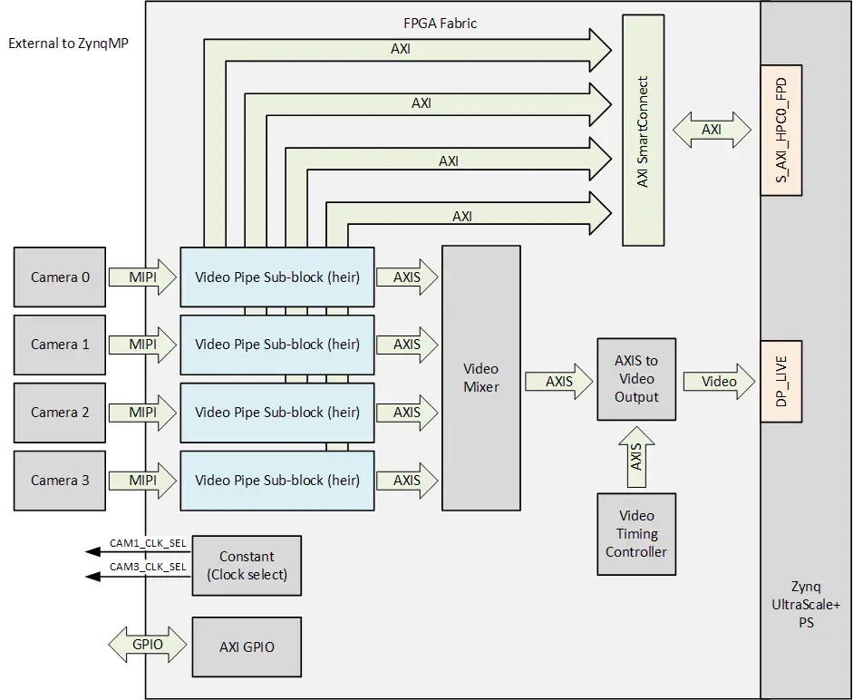
The main features illustrated in the block diagram are:
- Each camera has its own video pipe, a sub-block composed of multiple IPs which is described below.
- Each of the video pipes has 2x master AXI interfaces that connect to one of the high-performance slave interfaces on the PS, allowing for the video streams to be buffered in external high-bandwidth RAM.
- The output video streams are AXI-Streaming interfaces and they are input to a Video Mixer IP ( AMD Xilinx Video Mixer IP ) which combines them into a single video stream to be displayed on the DisplayPort monitor.
- The combined video stream is passed through the AMD Xilinx AXI4-Stream to Video Out IP to generate the video signals that are fed to the live DisplayPort interface of the ZynqMP.
- Timing signals for the AXIS to Video Out IP are generated by the AMD Xilinx Video Timing Controller IP .
- Constant outputs are provided for the clock select signals (CAM1_CLK_SEL and CAM3_CLK_SEL) to drive the MIPI switches, the values of which depend on the carrier board being used (see MIPI Switches for more detailed information on these pins).
- The AXI GPIO in the top level design is used to drive the DIR and OE_N inputs of the level translators to configure the direction of the camera IO0 and IO1 signals (see GPIO direction and output enable for more detailed information on these pins).
Video pipe
The video pipe sub-block diagram is illustrated below. We have again left out the AXI-Lite interfaces
and corresponding interconnect for clarity.
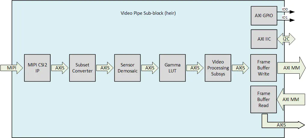
The main features of the video pipe are:
- The main input to the block is the MIPI CSI interface from the camera. This connects to the AMD Xilinx MIPI CSI Controller Subsystem IP which generates a RAW10 video stream on its AXI-Streaming interface.
- The first Subset Converter IP is used to truncate the RAW10 video stream to RAW8, using the most significant 8 bits of every pixel.
- The AMD Xilinx Sensor Demosaic IP converts the raw video stream to an RGB video stream by using an interpolation algorithm to calculate the missing color components for every pixel.
- The AMD Xilinx Gamma LUT IP performs gamma correction on the video stream.
- The AMD Xilinx Video Processor Subsystem IP allows for resolution scaling of the camera video streams.
- The Frame Buffer Write IP buffers the video stream into external high-bandwidth RAM.
- The Frame Buffer Read IP reads the video frames on the external high-bandwidth RAM and outputs them to an AXI-Streaming interface.
- Each video pipe has its own AXI GPIO for reading/writing it’s camera’s IO0 and IO1 pins. These are externalized in the top level design and are not shown in the top level block diagram for simplicity.
- Each video pipe also has its own AXI IIC for reading/writing to it’s camera’s I2C bus. These are externalized in the top level design and are not shown in the top level block diagram for simplicity.
Vision AI apps for ZCU10x Ubuntu 22.04 LTS
Description
These example designs demonstrate two smart vision apps that run on Certified Ubuntu 22.04 LTS for ZCU10x boards (for the ZCU10x boards only) or PetaLinux . These applications were designed by AMD Xilinx for the Kria KV260 platform and we ported them to the ZCU10x boards for use with the RPi Camera FMC. More detailed documentation regarding the applications can be found on the Kria KV260 Vision AI Starter Kit application documentation.
- Smartcam: An accelerated face detection application that supports RTSP network streaming output or DisplayPort output. This application can be used with a single Raspberry Pi camera connected to port CAM1 of the RPi Camera FMC.
- NLP Smart Vision: An accelerated face detection, object detection and plate detection application that uses Natural Language Processing to switch between AI tasks using verbal commands. This application can be used with one of two Raspberry Pi cameras connected to ports CAM1 and CAM2 of the RPi Camera FMC.
Links
Supported carrier boards
The Git repo contains an example design for each of the following carrier boards.
- AMD Xilinx ZCU104 Zynq UltraScale+ Development board
- AMD Xilinx ZCU102 Zynq UltraScale+ Development board
- AMD Xilinx ZCU106 Zynq UltraScale+ Development board
We are working on similar designs for the PYNQ-ZU, UltraZed-EV Carrier and Genesys-ZU boards.
Supported cameras
These example designs currently support the following cameras:
Support for more cameras will be added soon. We’re working hard on this and if you’d like to help us, please do. We accept pull requests on the Git repository.
Further documentation
The following tutorials have been written to help you get started building and using these example designs:
- Develop smart vision apps for ZCU106 and RPi Camera FMC
- NLP-SmartVision in PetaLinux on ZCU104 Using Raspberry Pi cameras
- Benchmarking an FPGA based AI Vision application
- A Smart Camera implemented in PetaLinux 2022.1 on ZCU104 Using a Raspberry Pi camera
Multi-cam ZynqMP and Hailo-8 AI Acceleration Demo
Description
This example design demonstrates a multi-camera YOLOv5 implementation that runs on the Zynq UltraScale+ and the Hailo-8 AI accelerator. The M.2 M-key Stack FMC is used to connect one or two Hailo-8 AI accelerators in M.2 M-key form factor, as well as the RPi Camera FMC and 4x Raspberry Pi Camera Module 2. The example design can be built for a few different Zynq UltraScale+ development boards (see below).
Links
Supported carrier boards
The Git repo contains an example design for each of the following carrier boards.
- AMD Xilinx ZCU104 Zynq UltraScale+ Development board
- AMD Xilinx ZCU106 Zynq UltraScale+ Development board
- TUL PYNQ-ZU Zynq UltraScale+ Development board
- Digilent Genesys-ZU Zynq UltraScale+ Development board
- Avnet UltraZed EV Carrier Zynq UltraScale+ Development board
The designs for some of these boards are limited to 2x cameras and some of them can only support 1x Hailo-AI module. For more information about these limitations, refer to the reference design documentation.