Detailed Description
Hardware Overview
The figure below illustrates the various hardware components that are located on the top-side of the RPi Camera FMC.
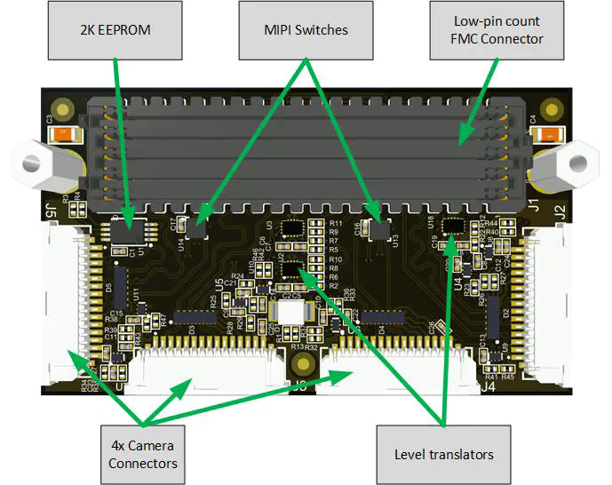
The main components on the top-side of the mezzanine card are:
- 4x 15-pin FFC connectors (camera connectors)
- Low Pin Count FMC Connector
- 2K EEPROM
- 2x MIPI switches
- Level translators
The figure below illustrates the various hardware components that are located on the bottom-side of the mezzanine card.
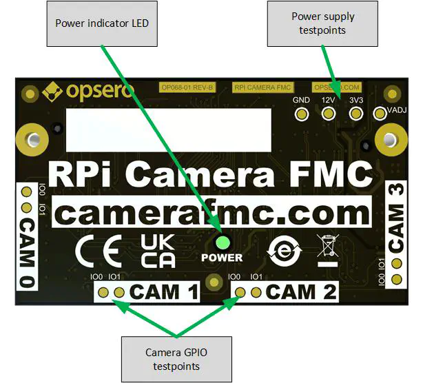
The main components on the bottom-side of the mezzanine card are:
- Power indicator LED
- Test points for power supplies
- Test points for camera GPIOs (IO0 and IO1)
Camera connectors
The Raspberry Pi cameras and compatible cameras connect to the mezzanine card through 4x 15-pin flat flexible cable (FFC) connectors.
The pinout of the camera connector is shown in the table below:
| Pin # | Signal name | Description |
|---|---|---|
| 1 | GND | Ground |
| 2 | DATA0_N | Data lane 0 (negative) |
| 3 | DATA0_P | Data lane 0 (positive) |
| 4 | GND | Ground |
| 5 | DATA1_N | Data lane 1 (negative) |
| 6 | DATA1_P | Data lane 1 (positive) |
| 7 | GND | Ground |
| 8 | CLK_N | Clock lane (negative) |
| 9 | CLK_P | Clock lane (positive) |
| 10 | GND | Ground |
| 11 | IO0 | General purpose IO 0 |
| 12 | IO1 | General purpose IO 1 |
| 13 | SCL | I2C bus clock |
| 14 | SDA | I2C bus data |
| 15 | 3V3 | 3.3VDC power supply |
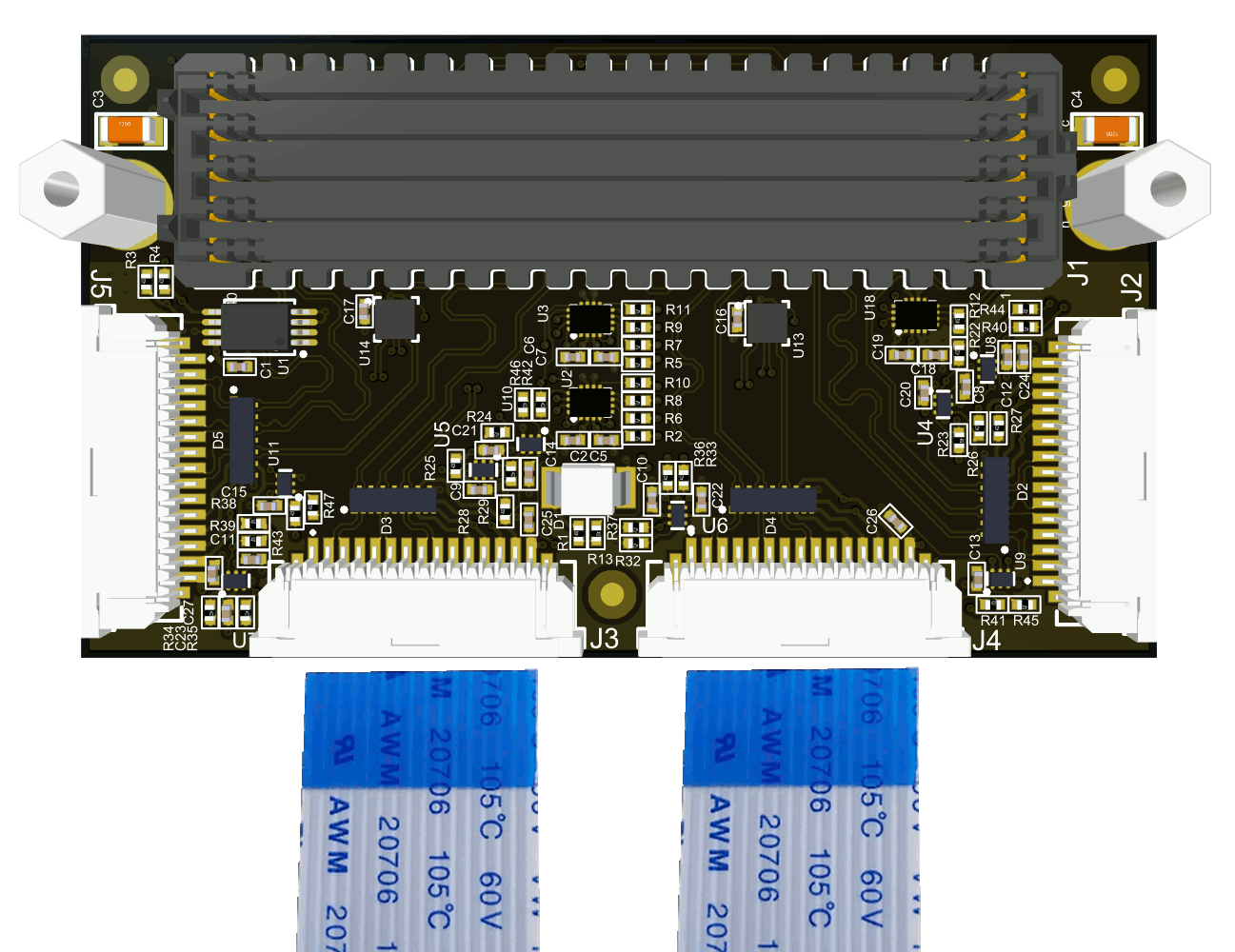
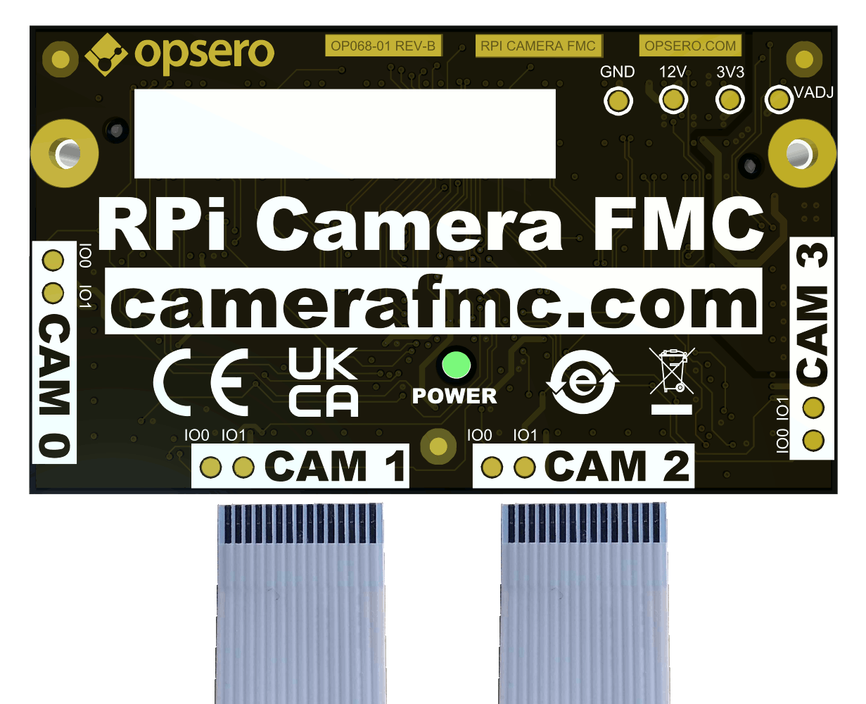
The camera connectors on the mezzanine card are Amphenol ICC, FFC connector, SFW15R-1STE1LF . This is a bottom contact connector, meaning that the flex cable of the camera must be inserted with the contacts facing downwards. The images below illustrate this requirement.
| Top view | Bottom view |
|---|---|
 |  |
EEPROM
The EEPROM ( ST, 2K EEPROM, M24C02-FDW6TP ) stores IPMI FRU data that can be read by the carrier board and contains the following information:
- Manufacturer name (Opsero Electronic Design Inc.)
- Product name
- Product part number
- Serial number
- Power supply requirements
The FRU data is read by some carrier boards to determine the correct VADJ voltage to apply to the mezzanine card. All Opsero FMC products have their EEPROMs programmed with valid FRU data to allow these carrier boards to correctly power them.
Low Pin Count FMC Connector
The RPi Camera FMC has a low pin count FMC (FPGA Mezzanine Card) connector for interfacing with an FPGA or SoC development board. The part number of this connector is Samtec, Low pin count FMC connector, ASP-134604-01 . The pinout of this connector conforms to the VITA 57.1 FPGA Mezzanine Card Standard (for more information, see Pin configuration. For more information on the FMC connector and the VITA 57.1 standard, see the Samtec page on VITA 57.1 .
Level translation
The FPGA I/O voltage (VADJ) is 1.2VDC however the Raspberry Pi camera I2C and GPIO interfaces require 3.3VDC signals. For this reason, the RPi Camera FMC uses bidirectional level translation devices to convert the VADJ voltage levels to 3.3VDC. The RPi Camera FMC uses the two devices listed below:
| Device | Purpose |
|---|---|
| TCA9416DTMR | Level translation of camera I2C buses. Always enabled. |
| SN74AVC4T245RSVR | Level translation of camera IO0, IO1. Direction and output enable are configurable. |
The level translation for the I2C buses is always enabled and cannot be configured. As for the camera GPIO, the user has some control over the direction of IO0 and IO1, as well as whether or not they enabled or disabled (see Camera GPIO for more information).
I/O Interfaces
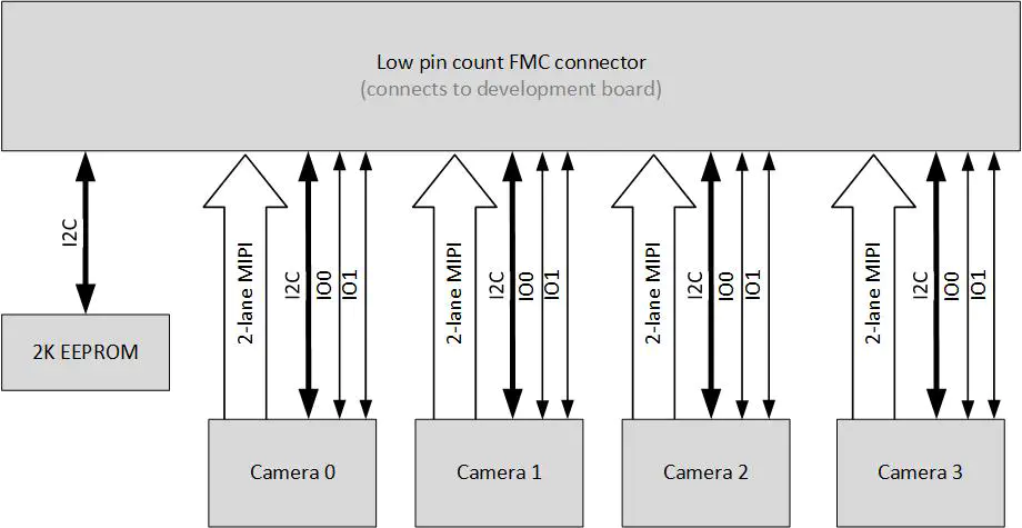
The FMC connector provides power to the RPi Camera FMC and also presents the following I/O signals to the FPGA fabric of the development board:
- 2-lane MIPI interfaces for each camera
- I2C buses (one for each camera)
- GPIO (IO0 and IO1) for each camera
- I2C for EEPROM R/W access
The MIPI interfaces, I2C buses and camera GPIO are routed to independent pins on the FMC connector. The figure below is a simplified connection diagram for the FMC connector. Note that the MIPI switches and level translation are left out of the diagram for clarity.
I2C Bus Interfaces
The I2C bus interface of each camera is routed independently to the FMC connector. In this configuration, there is no need for an I2C MUX, as the I2C buses are not linked together. Instead, each camera’s I2C bus is accessible through dedicated pins on the FMC connector, listed in the table below. This configuration simplifies the I2C interactions with the cameras, but comes at the expense of requiring a dedicated I2C controller for each camera to be implemented in the FPGA fabric.
| Camera | I2C signal | Net name | FMC pin |
|---|---|---|---|
| Camera 0 | SDA (data) | CAM0_SDA | LA03_P |
| SCL (clock) | CAM0_SCL | LA03_N | |
| Camera 1 | SDA (data) | CAM1_SDA | LA05_P |
| SCL (clock) | CAM1_SCL | LA05_N | |
| Camera 2 | SDA (data) | CAM2_SDA | LA30_P |
| SCL (clock) | CAM2_SCL | LA30_N | |
| Camera 3 | SDA (data) | CAM3_SDA | LA32_P |
| SCL (clock) | CAM3_SCL | LA32_N |
The I2C buses pass through level translators to convert the VADJ voltage levels to the 3.3VDC levels required by the Raspberry Pi cameras. These level translators are hard wired to be always enabled.
Camera GPIO
Eight FMC pins are dedicated to the control of each camera’s GPIO pins IO0 and IO1. These I/Os pass through level translators to convert the VADJ voltage levels to 3.3VDC levels required by the Raspberry Pi cameras.
| Camera | GPIO | Net name | FMC pin |
|---|---|---|---|
| Camera 0 | IO0 | CAM0_IO0 | LA12_N |
| IO1 | CAM0_IO1 | LA12_P | |
| Camera 1 | IO0 | CAM1_IO0 | LA09_N |
| IO1 | CAM1_IO1 | LA09_P | |
| Camera 2 | IO0 | CAM2_IO0 | LA19_N |
| IO1 | CAM2_IO1 | LA19_P | |
| Camera 3 | IO0 | CAM3_IO0 | LA20_N |
| IO1 | CAM3_IO1 | LA20_P |
Direction and output enable
Four FMC pins are dedicated for the configuration of the IO0 and IO1 direction and enabled state. These pins control the direction (camera-to-FPGA or FPGA-to-camera) and output enable for the IO0/IO1 signals, and the setting applies to all four cameras.
| Net name | FMC Pin | Purpose |
|---|---|---|
| CAM_IO0_DIR | LA13_P | IO0 direction (0=Cam-to-FPGA,1=FPGA-to-cam) |
| CAM_IO1_DIR | LA13_N | IO1 direction (0=Cam-to-FPGA,1=FPGA-to-cam) |
| CAM_IO0_OE_N | LA27_P | IO0 output enable (0=Enabled,1=Hi-Z output) |
| CAM_IO1_OE_N | LA27_N | IO1 output enable (0=Enabled,1=Hi-Z output) |
The diagram below illustrates the connection of the DIR and OE_N signals of the two level translators, one for IO0 and the other for IO1.
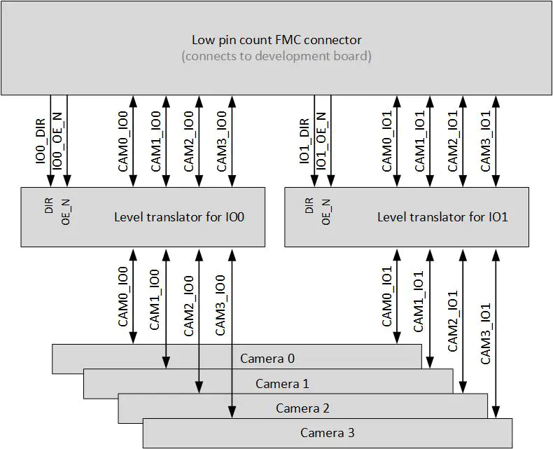
Note that in the case of the Raspberry Pi camera v2 and many of the compatible cameras, the IO0 should be configured as an output (FPGA-to-camera), while the IO1 can be left disabled. The usage of IO0 and IO1 on other cameras may be different and should be verified by the user.
| Camera | CAM_IO0_DIR | CAM_IO1_DIR | CAM_IO0_OE_N | CAM_IO1_OE_N |
|---|---|---|---|---|
| Raspberry Pi camera v2 | 1 | X 1 | 0 | X 1 |
| Digilent Pcam | 1 | X 1 | 0 | X 1 |
Testpoints
To facilitate debugging, testpoints for the GPIO (IO0 and IO1) of each camera is accessible on the bottom side of the mezzanine card. These testpoints are labelled in the bottom side view above.
MIPI Interfaces
The MIPI CSI interfaces from each camera are routed directly from the camera (FFC) connectors to the FMC connector. This is true for all of the MIPI signals with the exception of the MIPI clocks from cameras 1 and 3, which instead pass through MIPI switches (discussed in the following section). The MIPI CSI signals do not pass through any level translation on the RPi Camera FMC, therefore it is required that the carrier board’s FPGA device be able to receive MIPI CSI-2 D-PHY signals directly on it’s I/O pins. The AMD Xilinx UltraScale+ and Zynq UltraScale+ devices are capable of receiving MIPI CSI signals in this way.
MIPI Switches
To enable the RPi Camera FMC to support a useful range of carrier boards, it was designed with two MIPI switches ( OnSemi, MIPI Switch, FSA646AUCX ) that allow the MIPI clocks from cameras 1 and 3 to each be selectively routed to two different pairs on the FMC connector. The ability to redirect these camera clocks to suit the carrier board, allows the mezzanine card to support a wider range of carrier boards than would have otherwise been possible.
The diagram below illustrates the clock connections of cameras 1 and 3 through the MIPI switches. Note that the clock signals (shown as single thick lines for clarity) are actually differential and composed of a positive and negative trace.
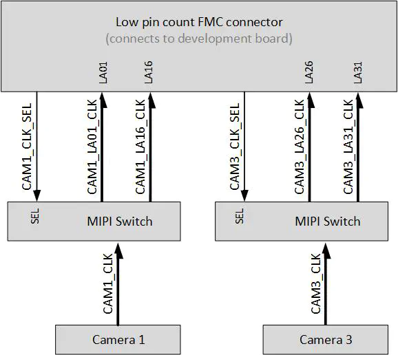
It is also important to note that all of the other MIPI signals, including the data lanes of cameras 1 and 3, as well as clock and data lanes of cameras 0 and 2, cannot be selectively routed as they connect directly from the FMC pins to the camera pins.
Two FMC pins are dedicated to driving the select (SEL) inputs of the MIPI switches; we refer to these signals as the clock select signals and they have the net names CAM1_CLK_SEL and CAM3_CLK_SEL. These signals pass through level converters before driving the MIPI switches which require 3.3VDC inputs. The table below shows the clock select signal locations on the FMC connector, and their effect on the routing of the clocks of cameras 1 and 3.
| Net name | FMC pin | Clock routing when CLK_SEL = 0 | Clock routing when CLK_SEL = 1 |
|---|---|---|---|
| CAM1_CLK_SEL | LA25_N | CAM1_CLK => LA01 | CAM1_CLK => LA16 |
| CAM3_CLK_SEL | LA25_P | CAM3_CLK => LA26 | CAM3_CLK => LA31 |
The clock select pins should be driven by the FPGA with constant values, depending on the carrier board that is being used. The table below lists the recommended clock select values for the currently supported carrier boards. Note that these required clock select values are included in the example designs.
| Dev board | CAM3_CLK_SEL | CAM1_CLK_SEL |
|---|---|---|
| ZCU104 | 1 | 0 |
| ZCU102 | 1 | 0 |
| ZCU106 | 1 | 0 |
| PYNQ-ZU | 1 | 0 |
| Genesys-ZU | 0 | 0 |
| UltraZed EV Carrier | 0 | 1 |
I/O Expanders
To facilitate production testing of this product, we designed it with 4x I/O expanders ( TI, I/O Expander, TCA9536DTMR ), one connected to the I2C bus of each camera. The I/O expanders have 4 I/Os, the first two of which are connnected to IO0 and IO1 through 510R resistors for protection in the event of bus contention. More information for using the I/O expanders can be found in the corresponding section of the programming guide.
Power Supplies
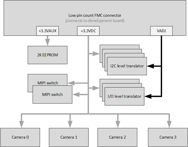
All power required by the RPi Camera FMC is supplied by the development board through the FMC connector:
- +12VDC
- +3.3VDC
- +3.3VAUX (for powering EEPROM only)
- VADJ: +1.2VDC
3.3VDC Supply
The 3.3VDC supply provides power for the 4x cameras, but it is also the supply for the MIPI switches and the level translators.
VADJ Supply
As the RPi Camera FMC uses level translators, it can be used with any VADJ voltage level between 1.2VDC and 3.3VDC without risk of damaging any of the components or the cameras. However, we strongly recommend using the RPi Camera FMC at the VADJ voltage level of 1.2VDC if you are using our example designs or other designs that are based on the AMD Xilinx MIPI CSI Controller Subsystem IP core.
The only devices on the RPi Camera FMC that are powered by the VADJ voltage, are the I2C level translators and the I/O level translators.
Power LED and testpoints
A single green LED on the RPi Camera FMC is used to indicate when the required power supplies are active. The LED is controlled by the PG pin of the FMC connector (driven by the carrier board), and driven by one of the I/O level translators.
To aid hardware debug, test points are accessible on the bottom side of the mezzanine card for each of the power supplies of the RPi Camera FMC.